Introduction
Semiconductor manufacturing is an extremely temperature-sensitive process, where even the smallest fluctuations in temperature can impact the quality, performance, and reliability of semiconductor devices. Microchips and integrated circuits (ICs) are produced using highly controlled fabrication processes, including photolithography, etching, deposition, ion implantation, and chemical mechanical planarization (CMP). Each of these steps requires precise thermal management to ensure uniformity, minimize defects, and enhance production yield. As semiconductor devices become smaller and more powerful, the need for accurate temperature control has increased. Advanced cooling and heating solutions, such as chillers, heat exchangers, liquid cooling systems, and thermoelectric modules, are implemented to maintain stable operating conditions in semiconductor fabrication plants (fabs). Additionally, semiconductor cleanrooms must have tight environmental controls, ensuring a consistent temperature and humidity to prevent contamination, material inconsistencies, and electrostatic discharge (ESD) damage.
Critical Areas Where Temperature Control is Essential
Photolithography and Etching
- Photolithography involves transferring circuit patterns onto silicon wafers using UV light exposure. Even a small temperature fluctuation can cause thermal expansion of wafers, leading to pattern misalignment and feature size variations.
- Deep UV (DUV) and Extreme UV (EUV) lithography require strict temperature regulation of the wafers, mask aligners, and light sources to maintain pattern accuracy and high-resolution imaging.
- Etching processes (wet and dry plasma etching) involve removing unwanted material from wafers. Temperature inconsistencies can lead to over-etching, under-etching, or non-uniform etching, affecting device performance.
Deposition Processes (CVD and PVD)
- Chemical Vapor Deposition (CVD) and Physical Vapor Deposition (PVD) are critical for layering dielectric, metal, and semiconductor materials onto wafers.
- Temperature variations during deposition can cause film thickness non-uniformity, void formation, and stress-induced defects, leading to performance issues in chips.
- High-precision temperature control systems ensure consistent film growth rates, leading to better electrical properties and improved chip durability.
Ion Implantation and Diffusion
- Ion implantation introduces dopants (such as phosphorus or boron) into silicon wafers to modify electrical properties.
- Temperature fluctuations during this process can lead to dopant clustering, unintended diffusion, and defects, reducing the efficiency of the semiconductor device.
- Diffusion furnaces, where wafers are heated to high temperatures for dopant activation, require strict thermal control to maintain uniform dopant distribution and optimal electrical characteristics.
Chemical Mechanical Planarization (CMP)
- CMP is used to polish and flatten wafer surfaces before subsequent processing steps.
- The slurries and polishing pads used in CMP must be maintained at consistent temperatures to prevent surface defects, dishing, and erosion.
- Advanced temperature control solutions in CMP systems enhance surface smoothness, improve planarization uniformity, and reduce production defects.
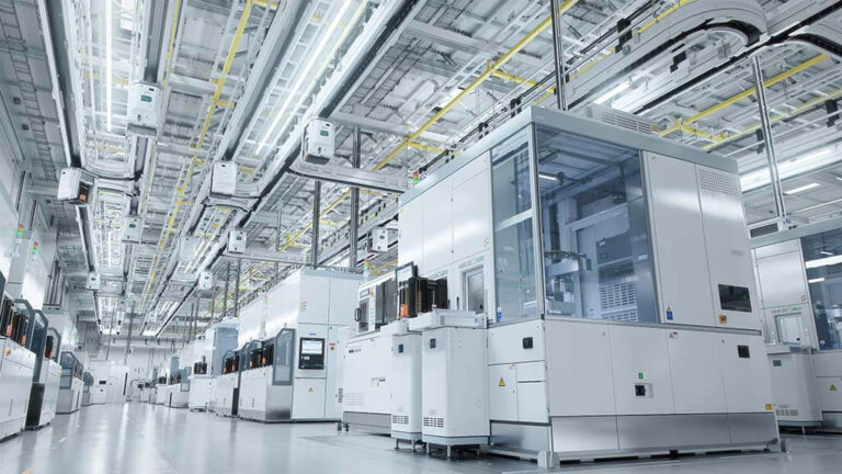
Cooling Solutions for Semiconductor Equipment
- Various semiconductor processing tools, including lasers, plasma etchers, and vacuum chambers, require precise cooling systems to avoid thermal damage and maintain efficiency.
- Chillers, heat exchangers, and liquid cooling systems (using deionized water, glycol mixtures, or refrigerants) help dissipate excess heat from equipment.
- Thermoelectric cooling (Peltier modules) provides localized, highly precise temperature control, essential for sensitive semiconductor applications.
Cleanroom Temperature and Humidity Control
- Semiconductor fabs operate in controlled cleanroom environments where temperature, humidity, and air quality must be maintained within narrow tolerances.
- Temperature control within ±0.1°C is required in advanced cleanrooms to prevent wafer warping, material expansion, and contamination.
- HVAC systems with HEPA and ULPA filters maintain cleanroom air quality and prevent moisture buildup, reducing the risk of electrostatic discharge (ESD) damage.
Thermal Management in Semiconductor Testing and Packaging
- After fabrication, semiconductors undergo rigorous testing under various temperature conditions to ensure they function correctly.
- Burn-in testing, where chips are exposed to elevated temperatures, ensures reliability in real-world applications.
- Temperature-controlled wafer probe stations and test chambers help identify defective chips before packaging, reducing overall waste.
Energy Efficiency and Sustainability in Thermal Management
- AI-driven thermal management solutions optimize cooling and heating based on real-time sensor data, reducing energy consumption.
- Recycling waste heat using heat recovery systems improves energy efficiency in fabs.
- Advanced cooling systems with low-GWP (Global Warming Potential) refrigerants support environmentally friendly semiconductor production.
Conclusion
Temperature control is a fundamental aspect of semiconductor manufacturing, influencing process precision, product yield, and device reliability. With nano-scale circuit architectures and high-speed computing chips, even the slightest temperature fluctuations can lead to significant defects and reduced performance. The industry is adopting cutting-edge thermal management technologies, such as AI-based cooling optimization, energy-efficient chillers, and next-generation thermoelectric solutions, to improve process stability, reduce downtime, and enhance sustainability. As semiconductor technology advances towards sub-2nm fabrication nodes, quantum computing, and AI-driven chip designs, high-precision temperature control systems will play a crucial role in enhancing efficiency, ensuring product quality, and meeting the growing demands of the electronics industry.